
1. Combinational Logic
1.1 Basic Gates
Wire
- question & answer
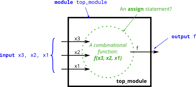
Implement the following circuit:

module top_module (
    input in,
    output out);
assign out = in;
endmodule
GND
- question & answer
Implement the following circuit:

module top_module (
    output out);
assign out = 1'b0;
endmodule
NOR
- question & answer
Implement the following circuit:

module top_module (
    input in1,
    input in2,
    output out);
    assign out = ~(in1|in2);
endmodule
Another gate
- question & answer
Implement the following circuit:

module top_module (
    input in1,
    input in2,
    output out);
    assign out = in1 & ~(in2);
endmodule
Two gates
- question & answer
Implement the following circuit:

module top_module (
    input in1,
    input in2,
    input in3,
    output out);
    assign out = (~(in1 ^ in2))^in3;
endmodule
More logic gates
- question & answer
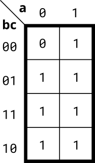
Build a combinational circuit with two inputs, a and b.
There are 7 outputs, each with a logic gate driving it: - out_and: a and b
- out_or: a or b
- out_xor: a xor b
- out_nand: a nand b
- out_nor: a nor b
- out_xnor: a xnor b
- out_anotb: a and-not b
module top_module(
    input a, b,
    output out_and,
    output out_or,
    output out_xor,
    output out_nand,
    output out_nor,
    output out_xnor,
    output out_anotb
);
    assign out_and = a&b;
    assign out_or = a|b;
    assign out_xor = a^b;
    assign out_nand = ~out_and;
    assign out_nor = ~out_or;
    assign out_xnor = ~out_xor;
    assign out_anotb = a&(~b);
endmodule
7420 chip
- question & answer
7400系列集成电路是一系列数字芯片,每个芯片都有几个门。 7420是一款带有两个4输入与非门的芯片。创建一个与 7420 芯片具有相同功能的模块。它有 8 个输入和 2 个输出。
Create a module with the same functionality as the 7420 chip. It has 8 inputs and 2 outputs.
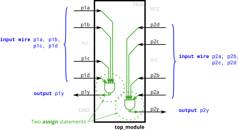
module top_module (
    input p1a, p1b, p1c, p1d,
    output p1y,
    input p2a, p2b, p2c, p2d,
    output p2y );
    assign p1y = ~(p1a&p1b&p1c&p1d);
    assign p2y = ~(p2a&p2b&p2c&p2d);
endmodule
Truth tables
- question & answer
创建一个实现真值表的组合电路。
Create a combinational circuit that implements the above truth table.
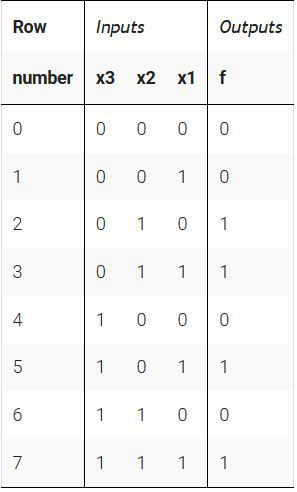
module top_module(
    input x3,
    input x2,
    input x1,  // three inputs
    output f   // one output
);
    assign f = ((~x3)&~(x1)&x2)|(x2&x1&(~x3))|(x3&x1&(~x2))|(x1&x2&x3);
endmodule
Two-bit equality
- question & answer
Create a circuit that has two 2-bit inputs A[1:0] and B[1:0], and produces an output z. The value of z should be 1 if A = B, otherwise z should be 0.
module top_module ( input [1:0] A, input [1:0] B, output z );
    assign z = (A == B)? 1'b1:1'b0;
endmodule
Simple circuit A
- question & answer
Module A is supposed to implement the function z = (x^y) & x. Implement this module.
module top_module (input x, input y, output z);
    assign z = (x^y)&x;
endmodule
Simple circuit B
- question & answer
实现输出如下波形的电路
Simple circuit A

module top_module ( input x, input y, output z );
    assign z = ~(x^y);
endmodule
Combine circuits A and B
- question & answer
See mt2015_q4a and mt2015_q4b for the submodules used here. The top-level design consists of two instantiations each of subcircuits A and B, as shown below.
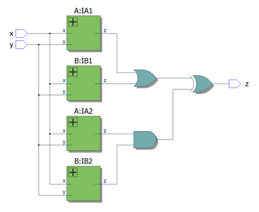
module top_module (input x, input y, output z);
    wire z1,z2,z3,z4;
    a a_instance1(
        .x(x),
        .y(y),
        .z(z1)
    );
    a a_instance2(
        .x(x),
        .y(y),
        .z(z3)
    );
    b b_instance1(
        .x(x),
        .y(y),
        .z(z2)
    );
    b b_instance2(
        .x(x),
        .y(y),
        .z(z4)
    );
    assign z = (z1|z2)^(z3&z4);
endmodule
module a (
    input wire x,
    input wire y,
    output wire z
);
    assign z = (x^y) & x;
endmodule

module b (
    input wire x,
    input wire y,
    output wire z
);
    assign z = ~x^y;
endmodule
Ring or vibrate
- question & answer
假设你正在设计一个电路来控制手机的振铃器和振动电机。当手机来电时(input ring),电路必须把震动( output motor = 1 )或响铃( output ringer = 1 )打开,但不能同时打开。当手机处于震动模式时( input vibrate = 1 ),则打开震动( output motor = 1 )。否则打开响铃。
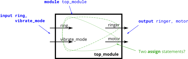
module top_module (
    input ring,
    input vibrate_mode,
    output ringer,       // Make sound
    output motor         // Vibrate
);
    assign motor = ring & vibrate_mode;
    assign ringer  = ring & (!vibrate_mode);

endmodule
Thermostat
- question & answer
一个冷/热恒温控制器可以同时在冬季和夏季对温度进行调节。设计一个电路,根据需要打开和关闭加热器、空调和鼓风机风扇。(本题可参照Problem 55 )
恒温器可以处于两种模式之一:制热(mode = 1)和制冷(mode = 0)。在制热模式下,当温度过低时(too_cold = 1),打开加热器,但不要使用空调。在制冷模式下,当温度过高(too_hot = 1)打开空调,但不要打开加热器。当加热器或空调打开时,也打开风扇使空气循环。此外,即使加热器和空调关闭,用户也可以请求将风扇打开(fan_on = 1)。
尝试仅使用assign语句来设计该电路,可参考上题
module top_module (
    input too_cold,
    input too_hot,
    input mode,
    input fan_on,
    output heater,
    output aircon,
    output fan
);
    assign heater = mode & too_cold;
    assign aircon = (~mode) & too_hot;
    assign fan = heater | aircon | fan_on;
endmodule
3-bit population count
- question & answer
“总体计数”电路计算输入向量中“1”的数量。为 3 位输入向量构建计数电路。
A “population count” circuit counts the number of ‘1’s in an input vector. Build a population count circuit for a 3-bit input vector.
module top_module(
    input [2:0] in,
    output [1:0] out );
    assign out = in[0] + in[1] + in[2];
endmodule
Gates and vectors
- question & answer
有一个4bit输入的电路,我们需要了解4bit输入数据之间的关系。 - out_both: 输入的每一个bit均需要检测该bit位与其左侧(即高比特位)是否全为 ‘ 1 ’ 。 示例:
out_both[2]应检测in[2]与in[3]是否均为 ‘ 1 ’ 。因为in[3]为输入的最高位,故我们无需检测out_both[3] - out_any: 输入的每一个bit均需要检测该bit位与其右侧(即低比特位)两者其中一个为 ‘ 1 ’ 。 示例:
out_any[2]应检测in[2]与in[1]两者其中一个为 ‘ 1 ’ 。因为in[0]为输入的最低位,故我们无需检测out_any[0] - out_different: 输入的每一个bit均需要检测该bit位与其左侧(即高比特位)两者是否不同。 示例:
out_different[2]应检测in[2]与in[3]两者是否不同 。在本节中,我们将输入变成一个环,所以in[3]的左侧为in[0]。
module top_module(
    input [3:0] in,
    output [2:0] out_both,
    output [3:1] out_any,
    output [3:0] out_different );
    assign out_both = in[2:0]&in[3:1];
    assign out_any = in[3:1]|in[2:0];
    assign out_different = in^{in[0],in[3:1]};
endmodule
Even longer vectors
- question & answer
该题与上题类似,仅将输入从4bit改为100bit ( input [99:0] ),题目的其余要求均相同。
TIPS
- out_both输出是判断现有bit位与其左侧bit位是否均为 ‘1’,可以采用移位运算来实现,
in[98] in[97] in[96] in[95] ……… in[3] in[2] in[1] in[0]
and
in[99] in[98] in[97] in[96] ……… in[4] in[3] in[2] in[1]
- out_any输出是判断现有bit位与右侧bit位两者间是否有一个为‘1’,也采用移位运算:
in[99]in[98]in[97]in[96]………in[4]in[3]in[2]in[1]
or
in[98]in[97]in[96]in[95]………in[3]in[2]in[1]in[0] - out_different输出同理,判断现有bit位与左侧bit位是否不同,唯一需要注意的是在此输出中题目要求将输入变为一个环,将in[0] 与 in[99] 链接在一起了,此处可采用链接符 { in[0], in[99:1] }。该输出同样采用移位运算。
in[99]in[98]in[97]in[96]………in[3]in[2]in[1]in[0]
xor
in[0]in[99]in[98]in[97]………in[4]in[3]in[2]in[1]module top_module( input [99:0] in, output [98:0] out_both, output [99:1] out_any, output [99:0] out_different ); assign out_both = in[98:0] & in[99:1]; assign out_any = in[99:1] | in[98:0]; assign out_different = in ^ {in[0],in[99:1]}; endmodule1.2 Multiplexers
Mux2to1
- question & answer
创建一个一位宽的 2 比 1 多路复用器。当sel=0时,选择a。当sel=1时,选择b。
Create a one-bit wide, 2-to-1 multiplexer. When sel=0, choose a. When sel=1, choose b.
module top_module(
    input a, b, sel,
    output out );
    assign out = sel?b:a;
endmodule
2 to 1 bus multiplexer
- question & answer
创建一个 100 位宽、2 比 1 多路复用器。当sel=0时,选择a。当sel=1时,选择b。
Create a 100-bit wide, 2-to-1 multiplexer. When sel=0, choose a. When sel=1, choose b.
module top_module(
    input [99:0] a, b,
    input sel,
    output [99:0] out );
    assign out = sel?b:a;
endmodule
9 to 1 bus multiplexer
- question & answer
创建一个 16 位宽、9 比 1 多路复用器。 sel=0 选择a,sel=1 选择b,等等。对于未使用的情况(sel=9 到15),将所有输出位设置为“1”。
Create a 16-bit wide, 9-to-1 multiplexer. sel=0 chooses a, sel=1 chooses b, etc. For the unused cases (sel=9 to 15), set all output bits to ‘1’.module top_module( input [15:0] a, b, c, d, e, f, g, h, i, input [3:0] sel, output [15:0] out ); always@(*)begin case(sel) 4'd0: out = a; 4'd1: out = b; 4'd2: out = c; 4'd3: out = d; 4'd4: out = e; 4'd5: out = f; 4'd6: out = g; 4'd7: out = h; 4'd8: out = i; default:out = 16'hffff; endcase end endmodule256 to 1 multiplexer
- question & answer
创建一个 1 位宽、256 比 1 多路复用器。 256 个输入全部打包到一个 256 位输入向量中。 sel=0 应选择 in[0] , sel=1 选择位 in[1] , sel=2 选择位 in[2] ,等等。
Create a 1-bit wide, 256-to-1 multiplexer. The 256 inputs are all packed into a single 256-bit input vector. sel=0 should select in[0], sel=1 selects bits in[1], sel=2 selects bits in[2], etc.
module top_module(
    input [255:0] in,
    input [7:0] sel,
    output out );
    assign out = in[sel];
endmodule
256 to 1 4bit multiplexer
- question & answer
创建一个 4 位宽、256 比 1 多路复用器。 256 个 4 位输入全部打包到一个 1024 位输入向量中。 sel=0 应选择位 in[3:0] ,sel=1 选择位 in[7:4] ,sel=2 选择位 in[11:8] 等。
Create a 4-bit wide, 256-to-1 multiplexer. The 256 4-bit inputs are all packed into a single 1024-bit input vector. sel=0 should select bits in[3:0], sel=1 selects bits in[7:4], sel=2 selects bits in[11:8], etc.
module top_module(
    input [1023:0] in,
    input [7:0] sel,
    output [3:0] out );
    //错误代码1
    //assign out[3:0] = in[(sel*4)+3 : sel*4];

    //错误代码2
  /*  always @(*)begin
        for(int sel = 0;sel<256;sel++)begin
            out[3:0] = in[(sel*4)+3 : sel*4];
        end
    end*/

    //正确代码
    assign out = {in[sel*4+3], in[sel*4+2], in[sel*4+1], in[sel*4+0]};
endmodule代码1和代码2的报错:Error (10734): Verilog HDL error at top_module.v(10): sel is not a constant
冒号“:”操作符:A[a : b]的含义理解为vectorA中选择位的范围,目前其中a和b只能是常数,而不能是变量。此处应该区分动态数组。
所以,应该将in[(sel4)+3:sel4]中的四个bit,用拼接符{}包括起来,{in[sel4+3], in[sel4+2], in[sel4+1], in[sel4+0]} 组成新的位宽为4的向量后再赋值给out。
多路选择器小结:在位宽较小的多路选择器中,我们可以使用 assign 语句,三元表达式,case 语句等。在位宽较宽的多路选择器中,需要根据需求灵活地使用位选择符或者位连接符。
HDLBits—笔记、难点、错题(1-5)case_mux, fadder, 卡诺图 – 知乎 (zhihu.com)
1.3 Arithmetic Circuits
Half adder
- question & answer
创建一个半加法器。半加器将两个位相加(没有进位输入)并产生总和和进位输出。
Create a half adder. A half adder adds two bits (with no carry-in) and produces a sum and carry-out.
写出真值表,可得出
cout = a&b;
sum = a^b
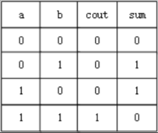
module top_module(
    input a, b,
    output cout, sum );
    assign cout = a&b;
    assign sum = a^b;
endmodule
Full adder
- question & answer
创建一个全加器。全加器将三位(包括进位输入)相加并产生总和和进位输出。
Create a full adder. A full adder adds three bits (including carry-in) and produces a sum and carry-out.
写出真值表,可以得出:
cout = a&b&(~cin) | a&(~b)&cin | b&cin;
sum = a^b^cin;
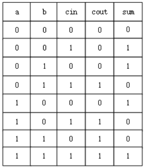
module top_module(
    input a, b, cin,
    output cout, sum );
    assign cout = a&b | a&cin | b&cin;
    assign sum = a^b^cin;
endmodule
Adder3
- question & answer
Now that you know how to build a full adder, make 3 instances of it to create a 3-bit binary ripple-carry adder. The adder adds two 3-bit numbers and a carry-in to produce a 3-bit sum and carry out. To encourage you to actually instantiate full adders, also output the carry-out from each full adder in the ripple-carry adder. cout[2] is the final carry-out from the last full adder, and is the carry-out you usually see.
例化三个一位全加器,实现三位全加器
module top_module(
    input [2:0] a, b,
    input cin,
    output [2:0] cout,
    output [2:0] sum );
    full_adder inst1(a[0],b[0],cin,cout[0],sum[0]);
    full_adder inst2(a[1],b[1],cout[0],cout[1],sum[1]);
    full_adder inst3(a[2],b[2],cout[1],cout[2],sum[2]);
endmodule

module full_adder(
    input a,
    input b,
    input cin,
    output cout,
    output sum
);
    assign cout = a&b | a&cin | b&cin;
    assign sum = a^b^cin;
endmodule
Exams/m2014 q4j
- question & answer
实现下面电路:
Implement the following circuit:
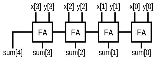
module top_module (
    input [3:0] x,
    input [3:0] y,
    output [4:0] sum);
    wire cout0,cout1,cout2;
    full_adder inst1(x[0],y[0],0,cout0,sum[0]);
    full_adder inst2(x[1],y[1],cout0,cout1,sum[1]);
    full_adder inst3(x[2],y[2],cout1,cout2,sum[2]);
    full_adder inst4(x[3],y[3],cout2,sum[4],sum[3]);
endmodule
module full_adder(
    input a,
    input b,
    input cin,
    output cout,
    output sum
);
    assign cout = a&b | a&cin | b&cin;
    assign sum = a^b^cin;
endmodule
或者
module top_module (
    input [3:0] x,
    input [3:0] y,
    output [4:0] sum);
    assign sum = x+y;
endmodule
Exams/ece241 2014 q1c
- question & answer
Assume that you have two 8-bit 2’s complement numbers, a[7:0] and b[7:0]. These numbers are added to produce s[7:0]. Also compute whether a (signed) overflow has occurred.
假设有两个8位的补码,a[7:0] 和 b[7:0]。 这些数字相加生成 s[7:0]。 还计算是否发生(有符号)溢出。
module top_module (
    input [7:0] a,
    input [7:0] b,
    output [7:0] s,
    output overflow
); //

     assign s = a+b;
    //两个数的补码相加,符号位参加运算,且两数和的补码等于两数的补码之和。

    //真值表得出  a  b  s  overflow
    //          0  0  1     1
    //          1  1  0     1
    assign overflow = a[7]&b[7]&(~s[7]) | (~a[7])&(~b[7])&s[7];
    //单符号——两符号相同的运算,运算结果符号相反的为溢出。
    //双符号法(变形补码法)——检测正负溢出

endmodule
TIPS:
单符号——两符号相同的运算,运算结果符号相反的为溢出。
Adder100
- question & answer
创建一个 100 位二进制加法器。加法器将两个 100 位数字和一个进位输入相加,产生 100 位sum和进位输出。
Create a 100-bit binary adder. The adder adds two 100-bit numbers and a carry-in to produce a 100-bit sum and carry out.
或者
module top_module(
    input [99:0] a, b,
    input cin,
    output cout,
    output [99:0] sum );
    assign {cout,sum} = a+b+cin;
endmodule
4-digit BCD adder
- question & answer
为您提供了一个名为 bcd_fadd 的 BCD(二进制编码的十进制)一位数加法器,它将两个 BCD 数字和进位相加,并产生总和和进位输出。
实例化 bcd_fadd 的 4 个副本以创建 4 位 BCD 纹波进位加法器。加法器应将两个 4 位 BCD 数字(打包为 16 位向量)和一个进位输入相加,以产生 4 位sum和进位输出。module top_module ( input [15:0] a, b, input cin, output cout, output [15:0] sum ); wire cout0,cout1,cout2; bcd_fadd bcd_fadd_inst1(a[3:0],b[3:0],cin,cout0,sum[3:0]); bcd_fadd bcd_fadd_inst2(a[7:4],b[7:4],cout0,cout1,sum[7:4]); bcd_fadd bcd_fadd_inst3(a[11:8],b[11:8],cout1,cout2,sum[11:8]); bcd_fadd bcd_fadd_inst4(a[15:12],b[15:12],cout2,cout,sum[15:12]); endmodule
1.4 Karnaugh Map to Circuit
3-variable
- question & answer
实现下面卡诺图描述的电路。
module top_module(
    input a,
    input b,
    input c,
    output out  );
    assign out = a|b|c;
endmodule
4-variable
- question & answer
实现下面卡诺图描述的电路。
module top_module(
    input a,
    input b,
    input c,
    input d,
    output out  );
    assign out = (~a)&(~d)||(~b)&(~c)||(~a)&b&c||b&c&d||a&c&d;
endmodule
4-variable
- question & answer
实现下面卡诺图描述的电路。
module top_module(
    input a,
    input b,
    input c,
    input d,
    output out  );
    assign out = ((~b)&c)||a;
endmodule
4-variable
- question & answer
实现下面卡诺图描述的电路。
module top_module(
    input a,
    input b,
    input c,
    input d,
    output out  );
    assign out = (a^b)^(c^d);
endmodule
Minimum SOP and POS
- TIPS
SOP(Sum of Products,最小项和表达)和POS(Product of Sums,最大项和表达)形式的逻辑函数分别通过最小项和最大项来获得。
SOP形式是找出所有当输出为1(最小项)的输入组合(乘积和)
POS则是找出所有当输出为0(最大项)的输入组合(和乘积)
如下进行SOP形式的逻辑函数表示:
| A | B | Y | min |
|---|---|---|---|
| 0 | 0 | 0 | |
| 0 | 1 | 1 | ~A&B |
| 1 | 0 | 0 | 0 |
| 1 | 1 | 1 | A&B |
由此 SOP形式的逻辑函数:
F = (~A&B) | (A&B )
如下进行POS形式的逻辑函数表示:
| A | B | Y | max |
|---|---|---|---|
| 0 | 0 | 0 | A + B |
| 0 | 1 | 1 | |
| 1 | 0 | 0 | ~A + B |
| 1 | 1 | 1 |
由此 POS形式的逻辑函数:
F = (A + B)& (~A + B)
- question & answer
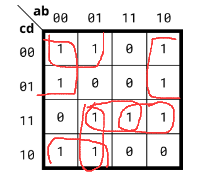
设计一个单输出的数字系统,该系统有四个输入(a, b, c, d)。题目给出了在某些输入条件下输出为逻辑1,在其他输入条件下输出为逻辑0,同时还有一些输入条件不会在系统中出现(即无关项)。
输入的组合可以表示为4位二进制数,对应如下: - 当输入是2、7、15时,输出为逻辑1。
- 当输入是0、1、4、5、6、9、10、13、14时,输出为逻辑0。
- 输入3、8、11、12不会出现(无关项)。
分别画出SOP、POS的卡诺图如下:
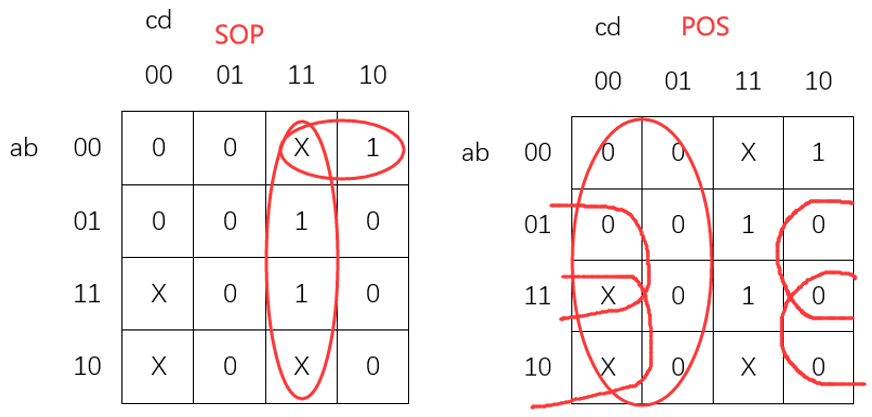
module top_module (
    input a,
    input b,
    input c,
    input d,
    output out_sop,
    output out_pos
);
    assign out_sop = c&d|(~a)&(~b)&c;
    assign out_pos = ~((~c)|b&(~d)|a&(~d));
endmodule
Kamaugh map
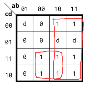
- question & answer
考虑下面卡诺图中显示的函数 f。实现这个功能。 d 是无关的,这意味着您可以选择输出任何方便的值。
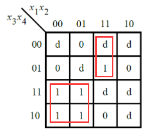
module top_module (
input [4:1] x,
output f );
assign f= (~x[1])&x[3]|x[1]&x[2]&(~x[3]);
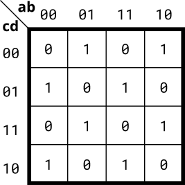
endmoduleKamaugh map
- question & answer
考虑下面卡诺图中显示的函数 f。实现这个功能。
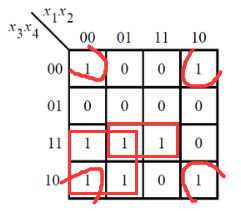
module top_module (
    input [4:1] x,
    output f
);
    assign f = (!x[2])&(~x[4])|(~x[1])&x[3]|x[2]&x[3]&x[4];
endmodule
K-map implemented witha multiplexer
- question & answer
对于下面的卡诺图,给出使用一个 4 对 1 多路复用器和所需数量的 2 对 1 多路复用器的电路实现,但使用的数量尽可能少。您不能使用任何其他逻辑门,并且必须使用 a 和 b 作为多路复用器选择器输入,如下面的 4 选 1 多路复用器所示。
您仅实现标记为 top_module 的部分,以便整个电路(包括 4-to-1 mux)实现 K-map。

module top_module (
    input c,
    input d,
    output [3:0] mux_in
);
    assign mux_in[0] = c|d;
    assign mux_in[1] = 0;
    assign mux_in[2] = ~d;
    assign mux_in[3] = c&d;
endmodule
2. Sequential Logic
2.1 Latches and Flip-Flops
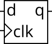
D flip-flop
- question & answer
D触发器是一种电路,用于存储一个比特,并定期在(通常是)时钟信号的正边沿进行更新。D触发器是逻辑综合器在使用时钟always块时创建的。D触发器是“组合逻辑块后跟一个触发器”的最简形式,其中组合逻辑部分只是一根导线。
创建单个 D 触发器
module top_module (
    input clk,    // Clocks are used in sequential circuits
    input d,
    output reg q );//
    always@(posedge clk)begin
       q<=d;
    end
endmodule
D flip-flops
创建 8 个 D 触发器。所有 DFF 应由 clk 的上升沿触发。
- question & answer
module top_module (
input clk,
input [7:0] d,
output [7:0] q
);
always@(posedge clk)begin
   q<=d;
end
endmodule
DFF with reset
- question & answer
创建具有高电平有效同步复位的 8 个 D 触发器。所有 DFF 应由 clk 的上升沿触发。module top_module ( input clk, input reset, // Synchronous reset input [7:0] d, output [7:0] q ); always@(posedge clk)begin if(reset) q<='d0; else q<=d; end endmodule
DFF with reset value
- question & answer
创建具有高电平有效同步复位的 8 个 D 触发器。触发器必须重置为 0x34 而不是零。所有 DFF 均应由 clk 的下降沿触发。module top_module ( input clk, input reset, input [7:0] d, output [7:0] q ); always@(negedge clk)begin if(reset) q<=8'h34; else q<=d; end endmoduleDFF with asynchronous reset
- question & answer
创建具有高电平有效异步复位的 8 个 D 触发器。所有 DFF 应由 clk 的上升沿触发。module top_module ( input clk, input areset, // active high asynchronous reset input [7:0] d, output [7:0] q ); always@(posedge clk or posedge areset)begin if(areset) q<='d0; else q<=d; end endmoduleDFF with byte enable
- question & answer
创建16个D触发器。有时仅修改一组触发器的部分。字节使能输入控制是否在该周期写入16个寄存器中的每个字节。byteena[1]控制高字节d[15:8],而byteena[0]控制低字节d[7:0]。
resetn 是同步、低电平有效复位。所有 DFF 应由 clk 的上升沿触发。module top_module ( input clk, input resetn, input [1:0] byteena, input [15:0] d, output [15:0] q ); always@(posedge clk)begin if(!resetn) q<='d0; else begin if(byteena[0]) q[7:0]<=d[7:0]; if(byteena[1]) q[15:8]<=d[15:8]; end end endmoduleDLatch
- question & answer
实现以下电路(请注意,这是一个锁存器,因此 Quartus 会出现有关推断锁存器的警告。):
module top_module (
    input d,
    input ena,
    output q);
    always@(*)begin
        if(ena)
            q<=d;
    end
endmodule
DFF
- question & answer
实现下面电路
module top_module (
    input clk,
    input d,
    input ar,   // asynchronous reset
    output q);
    always@(posedge clk or posedge ar)begin
        if(ar)
            q<='d0;
        else
            q<=d;
    end
endmodule
DFF
- question & answer
实现下面电路
module top_module (
    input clk,
    input d,
    input r,   // synchronous reset
    output q);
    always@(posedge clk)begin
        if(r)
            q<='d0;
        else
            q<=d;
    end
endmodule
DFF+gate
- question & answer
实现下面电路:

module top_module (
    input clk,
    input in,
    output out);
    always@(posedge clk)begin
        out<=(in^out);
    end
endmodule
Mux and DFF
考虑下面的时序电路:假设您想要为此电路实现分层 Verilog 代码,使用其中包含触发器和多路复用器的子模块的三个实例。为此子模块编写一个名为 top_module 的Verilog模块(包含一个触发器和多路复用器)。

- question & answer
module top_module (
    input clk,
    input L,
    input r_in,
    input q_in,
    output reg Q);
    wire mux_out;
    always@(*)begin
        case(L)
            1'b0:mux_out = q_in;
            1'b1:mux_out = r_in;
        endcase
    end
    always@(posedge clk)begin
        Q<=mux_out;
    end
endmodule
Mux and DFF
考虑如下所示的 n 位移位寄存器电路,为该电路的一级编写一个名为 top_module 的 Verilog 模块,包括触发器和多路复用器。

- question & answer
module top_module (
input clk,
input w, R, E, L,
output Q
);
wire mux_out1,mux_out2;
always@(*)begin
    case(E)
        1'b0:mux_out1=Q;
        1'b1:mux_out1=w;
    endcase
    case(L)
        1'b0:mux_out2=mux_out1;
        1'b1:mux_out2=R;
    endcase
end
always@(posedge clk)begin
    Q<=mux_out2;
end
endmodule
DFFs and gates
- question & answer
给定如图所示的有限状态机电路,假设 D 触发器在机器开始之前最初重置为零。搭建这个电路。
module top_module (
    input clk,
    input x,
    output z
);
    wire d1,d2,d3;
    wire q1,q2,q3;
    always@(*)begin
        d1 = x^q1;
        d2 = x&(~q2);
        d3 = x|(~q3);
        z = ~(q1|q2|q3);
    end
    always@(posedge clk)begin
        q1<=d1;
        q2<=d2;
        q3<=d3;
    end
endmodule
Create circuit from truth table
- question & answer
JK 触发器具有以下真值表。仅使用 D 型触发器和门实现 JK 触发器。注:Qold 是时钟正沿之前 D 触发器的输出。
| J | K | Q |
|---|---|---|
| 0 | 0 | Qold |
| 0 | 1 | 0 |
| 1 | 0 | 1 |
| 1 | 1 | ~Qold |
module top_module (
    input clk,
    input j,
    input k,
    output Q);
    always@(posedge clk)begin
        case({j,k})
            2'b00:Q<=Q;
            2'b01:Q<=0;
            2'b10:Q<=1;
            2'b11:Q<=~Q;
        endcase
    end
endmodule
Detect an edge
- question & answer
对于 8 位向量中的每一位,检测输入信号何时从一个时钟周期内的 0 变为下一个时钟周期内的 1(类似于正边沿检测)。应在 0 到 1 转换发生后的周期设置输出位。
module top_module (
    input clk,
    input [7:0] in,
    output [7:0] pedge
);
    wire [7:0] in_delay;
    always@(posedge clk)begin
        in_delay <= in;
    end
    always@(posedge clk)begin
        pedge <= in&~in_delay; //检测in(1)前一个in(0)即可
    end
endmodule
Detect both edges
- question & answer
对于 8 位向量中的每一位,检测输入信号何时从一个时钟周期更改为下一个时钟周期(检测任何边沿)。应在 0 到 1 转换发生后的周期设置输出位。module top_module ( input clk, input [7:0] in, output [7:0] anyedge ); wire [7:0]in_delay; always@(posedge clk)begin in_delay <= in; anyedge <= in^in_delay; //检测信号前后相异 end endmoduleEdge capture register
- question & answer
探测输入信号每一位的下降沿,若其中部分位有下降沿,则下一周期输出对应位高电平并锁存,直到复位信号reset到来才复位为0。
module top_module (
    input clk,
    input reset,
    input [31:0] in,
    output [31:0] out
);
    wire [31:0]in_delay;
    always@(posedge clk)begin
        in_delay<=in;
    end
    always@(posedge clk)begin
        if(reset)
            out <= 'd0;
        else
            out <= ~in&in_delay | out;//如果不与 out 相或,每个时钟周期 out 都会被重新计算
    end
endmodule
Dual-edge triggered flip-flop
- question & answer
由于FPGA不支持双边沿触发触发器,我们需要通过其他方式来模拟双边沿触发行为。
module top_module(
    input clk,
    input d,
    output q
);

    reg p, n;  // 定义两个寄存器 p 和 n 分别用于捕捉上升沿和下降沿的信号
    // 上升沿触发的触发器
    always @(posedge clk)
        p <= d ^ n;  // 在时钟的上升沿,p 更新为 d 和 n 的异或
    // 下降沿触发的触发器
    always @(negedge clk)
        n <= d ^ p;  // 在时钟的下降沿,n 更新为 d 和 p 的异或
    // 输出 q 是 p 和 n 的异或
    assign q = p ^ n;
endmodule
2.2 Counters
Four-bit binary counter
- question & answer
构建一个 4 位二进制计数器,从 0 到 15(含)计数,周期为 16。复位输入是同步的,应将计数器复位为 0。module top_module ( input clk, input reset, // Synchronous active-high reset output [3:0] q); always@(posedge clk)begin if(reset || q==4'd15) q<='d0; else q<=q+1; end endmoduleDecade counter
- question & answer
构建一个从 0 到 9(含)的十进制计数器,周期为 10。复位输入是同步的,应将计数器复位为 0。module top_module ( input clk, input reset, // Synchronous active-high reset output [3:0] q); always@(posedge clk)begin if(reset || q==4'd9) q<='d0; else q<=q+1; end endmoduleDecade counter again
- question & answer
制作一个十年计数器,从 1 到 10(含 1 和 10)。复位输入是同步的,并且应该将计数器复位为 1。module top_module ( input clk, input reset, output [3:0] q); always@(posedge clk)begin if(reset || q==4'd10) q<='d1; else q<=q+1; end endmoduleslow decade counter
- question & answer
构建一个从 0 到 9(含)的十进制计数器,周期为 10。复位输入是同步的,并且应该将计数器重置为 0。我们希望能够暂停计数器,而不是总是在每个时钟周期递增,因此 slowena 输入指示计数器何时应递增。module top_module ( input clk, input slowena, input reset, output [3:0] q); always@(posedge clk)begin if(reset) q<='d0; else if(slowena)begin if(q==4'd9) q<=0; else q<=q+1; end end endmodule
Counter 1-12
- question & answer
设计一个1到12的计数器,具有以下输入和输出:- 复位(Reset):同步高电平复位,将计数器强制复位为1。
- 使能(Enable):设置为高,启动计数器。
- 时钟(Clk):正边沿触发时钟输入。
- Q[3:0]:计数器的输出。
- c_enable, c_load, c_d[3:0]:控制信号传输给提供的4位计数器,以验证正确操作。
可以使用以下组件: - 提供的4位二进制计数器(count4),具有使能和同步并行加载输入(load优先级高于enable)。count4模块已经提供。请在电路中实例化它。
- 逻辑门。
module count4(
input clk,
input enable,
input load,
input [3:0] d,
output reg [3:0] Q
);
- c_enable、c_load和c_d输出分别是传输到内部计数器的使能、加载和数据输入的信号。它们的目的是允许检查这些信号的正确性。
module top_module (
input clk,
input reset,
input enable,
output [3:0] Q,
output c_enable,
output c_load,
output [3:0] c_d
);

// count4 the_counter (.clk(clk), .(c_enable), .c_load, .c_d /*, ... */ );
assign c_enable = enable;
assign c_load = reset | ((Q == 4'd12) && (enable == 1'b1));
assign c_d = c_load ? 4'b1:4'b0;
count4 u1(.clk(clk),.enable(c_enable),.load(c_load),.d(c_d),.Q(Q));
endmodule
Counter 1000
- question & answer
从一个1000 Hz的时钟信号中派生出一个1 Hz的信号,称为OneHertz,用于驱动一组小时/分钟/秒计数器的使能信号,从而创建一个数字wall clock。由于我们希望时钟每秒钟计数一次,因此OneHertz信号必须每秒精确地保持高电平一个时钟周期。使用尽可能少的其他门电路来构建频率分频器,使用模10(BCD)计数器。同时输出你使用的每个BCD计数器的使能信号(c_enable[0]表示最快的计数器,c_enable[2]表示最慢的计数器)。
已经为你提供了以下BCD计数器。使能信号必须保持高电平以使计数器运行。复位是同步的,将其置为高可强制计数器清零。你的电路中的所有计数器必须直接使用相同的1000 Hz信号。
module bcdcount (
    input clk,
    input reset,
    input enable,
    output reg [3:0] Q
);
module top_module (
input clk,
input reset,
output OneHertz,
output [2:0] c_enable
); //
wire [3:0] one,ten,hundred;
assign c_enable = {one == 4'd9 && ten == 4'd9,one == 4'd9,1'd1};
assign OneHertz = {one == 4'd9 && ten == 4'd9 && hundred == 4'd9};
bcdcount counter0 (clk, reset, c_enable[0],one);
bcdcount counter1 (clk, reset, c_enable[1],ten);
bcdcount counter2 (clk, reset, c_enable[2],hundred);
endmodule4-digit decimal counter
- question & answer
构建一个 4 位数的 BCD(二进制编码的十进制)计数器。每个十进制数字使用4位进行编码:q[3:0]是1位,q[7:4]是十位,依此类推。对于数字 [3:1],还要输出一个使能信号,指示上三位数字中的每一位何时应递增。
您可能希望实例化或修改一些一位数的十计数器。module top_module ( input clk, input reset, // Synchronous active-high reset output [3:1] ena, output [15:0] q); reg [3:0] one,ten,hundred,thousand; always @(posedge clk) begin if(reset || (one == 4'd9)) one <= 4'b0; else one <= one +1'b1; end always @(posedge clk) begin if(reset || ((ten == 4'd9) && (one == 4'd9))) ten <= 4'b0; else if(one == 4'd9) ten <= ten +1'b1; end always @(posedge clk) begin if(reset || ((ten == 4'd9) &&( one == 4'd9) && (hundred == 4'd9))) hundred <= 4'b0; else if((ten == 4'd9) &&( one == 4'd9)) hundred <= hundred +1'b1; end always @(posedge clk) begin if(reset || ((ten == 4'd9) &&( one == 4'd9 )&& (hundred == 4'd9) &&( thousand == 4'd9))) thousand <= 1'b0; else if((ten == 4'd9) &&( one == 4'd9 )&& (hundred == 4'd9)) thousand <= thousand +1'b1; end assign q = {thousand,hundred,ten,one}; assign ena[1] = (one == 4'd9) ? 1'b1:1'b0; assign ena[2] = ((one == 4'd9) && (ten == 4'd9)) ? 1'b1:1'b0; assign ena[3] = ((one == 4'd9) && (ten == 4'd9) && (hundred == 4'd9)) ? 1'b1:1'b0; endmodule
12-hour clock
- question & answer
创建一组适合用作 12 小时制的计数器(带 am/pm 指示器)。您的计数器由快速运行的clk计时,只要您的时钟应该增加(即每秒一次),就会在ena上发出脉冲。
Reset将时钟重置为 12:00 AM。pm 表示 AM 为 0,PM 为 1。hh、mm 和 ss 是两个 BCD(二进制编码十进制)数字,分别表示小时 (01-12)、分钟 (00-59) 和秒 (00-59)。Reset的优先级高于enable,即使未enable,也可能发生Reset。
以下时序图显示了从上午 11:59:59 到中午 12:00:00 的翻转行为以及同步复位和使能行为。
//在顶层模块中实现例化
module top_module(
    input clk,
    input reset,
    input ena,
    output pm,
    output [7:0] hh,
    output [7:0] mm,
    output [7:0] ss);
    count60 u1(.clk(clk),.reset(reset),.en(ena),.cnt_out(ss));//秒
    count60 u2(.clk(clk),.reset(reset),.en(ena&(ss==8'h59)),.cnt_out(mm));//分
    count12 u3(.clk(clk),.reset(reset),.en(ena&(ss==8'h59)&(mm===8'h59)),.cnt_out(hh));//时
    reg pm1;
    always @(posedge clk)
        begin
            if(reset)
                pm1 <= 8'h0;
            else if((hh == 8'h11)&(ss == 8'h59)&(mm == 8'h59))
                pm1 <= ~pm1;
            else;
        end
    assign pm =pm1;
endmodule
//设计0-59的模60计数器
module count60(clk,reset,en,cnt_out);
    input clk,reset,en;
    output reg [7:0] cnt_out;
    always @(posedge clk)
        begin
            if(reset)
                cnt_out <= 8'h0;
            else if(en)
                if(cnt_out == 8'h59)begin
                    cnt_out <= 8'h0;
                end
            else if(cnt_out[3:0] == 9)begin
                cnt_out[3:0] <= 0;
                cnt_out[7:4] <= cnt_out[7:4] + 1;//bcd计数器实现的递增
            end
            else

                cnt_out[3:0] <= cnt_out[3:0] + 1;
        end
endmodule
//设计模12的计数器
module count12(clk,en,reset,cnt_out);
    input clk,en,reset;
    output cnt_out;
    reg [7:0] cnt_out;
    always @(posedge clk)
        begin
            if(reset)
                cnt_out <= 8'h12;//题意要求复位有效时复位至12点
            else if(en)
                begin
                    if(cnt_out == 8'h12)
                        begin
                            cnt_out <= 1;
                        end
                    else if(cnt_out[3:0] == 9)
                        begin
                       cnt_out[3:0] <= 0;
                       cnt_out[7:4] <= cnt_out[7:4] + 1;//bcd计数器实现的递增
                        end
                    else
                        begin
                            cnt_out[3:0] <= cnt_out[3:0] + 1;
                        end
                end
        end
endmodule
2.3 Shift Registers
4-bit shift register
- question & answer
构建一个 4 位移位寄存器(右移),具有异步复位、同步加载和使能功能。
areset :将移位寄存器重置为零。
load :使用 data[3:0] 加载移位寄存器而不是移位。
ena :右移( q[3] 变为零, q[0] 移出并消失)。
如果 load 和 ena 输入均已置位 (1),则 load 输入具有更高的优先级。
q :移位寄存器的内容。module top_module( input clk, input areset, // async active-high reset to zero input load, input ena, input [3:0] data, output reg [3:0] q); always@(posedge clk or posedge areset)begin if(areset) q<='d0; else if(load) q<=data; else if(ena)begin q[0]<=q[1]; q[1]<=q[2]; q[2]<=q[3]; q[3]<=1'b0; //q <= {1'b0,q[3:1]}; end else q<=q; end endmodule
Left/right rotator
- question & answer
构建一个具有同步加载、左/右旋转使能的100位左/右旋转器(其实就是循环移位寄存器)。旋转器从寄存器的另一端将移出的位移入,与只舍弃移出位并移入零的移位器不同。如果启用,旋转器会将位在寄存器中旋转,而不是修改或舍弃它们。
load :使用 data[99:0] 加载移位寄存器而不是旋转。
ena[1:0] :选择是否旋转以及旋转方向。- 2’b01 右移一位
- 2’b10 左移一位
- 2’b00 和 2’b11 不旋转。
q :旋转器的内容。module top_module( input clk, input load, input [1:0] ena, input [99:0] data, output reg [99:0] q); always@(posedge clk)begin if(load) q<=data; else begin case(ena) 2'b10:q<={q[98:0],q[99]}; 2'b01:q<={q[0],q[99:1]}; default:q<=q; endcase end end endmodule
Left/right arithmetic shift1 or 8
- question & answer
构建一个64位算术移位寄存器,带有同步加载功能。这个移位器可以向左和向右移动,移动的位数可以是1位或8位,根据指定的amount来选择。
算术右移会将位移寄存器中的符号位(在这种情况下是q[63])移入,而不像逻辑右移那样移入0。另一种理解算术右移的方式是,它假设被移动的数字是有符号的,并且保留符号,因此算术右移相当于将有符号数除以2的幂次方。
逻辑左移和算术左移之间没有区别。
load:用data[63:0]加载移位寄存器,而不进行移位。
ena:选择是否进行移位操作。
amount:选择移动的方向和位数。
2’b00:向左移动1位。
2’b01:向左移动8位。
2’b10:向右移动1位。
2’b11:向右移动8位。
q:移位寄存器的内容。module top_module( input clk, input load, input ena, input [1:0] amount, input [63:0] data, output reg [63:0] q); always@(posedge clk)begin if(load) q<=data; else if(ena)begin case(amount) 2'b00:q<={q[62:0],1'b0}; 2'b01:q<={q[55:0],8'b0}; 2'b10:q<={q[63],q[63:1]}; 2'b11:q<={{8{q[63]}},q[63:8]}; endcase end else q<=q; end endmodule
5-bit LFSR
- TIPS
线性反馈移位寄存器可参考这篇:详解线性反馈移位寄存器(LFSR)-CSDN博客- question & answer
线性反馈移位寄存器,即linear feedback shift register(LFSR),是通常带有几个XOR门的移位寄存器,以产生移位寄存器的下一个状态。 Galois LFSR是一种特殊的设置,其中带有“抽头tap”的位与输出位进行异或运算以产生其下一个值,而没有移动“tap”位位置。如果仔细选择tap位置,LFSR可以设为“最大长度”。n位的最大长度LFSR在重复之前循环经过2n-1个状态(永远不会达到全零状态)。
下图显示了一个5位最大长度的Galois LFSR,在位置5和3处有抽头,即tap(抽头“tap”位置通常从1开始编号)。
请注意,为保持一致性,在位置5处绘制了XOR门,但XOR门输入之一为0。
构建这个 LFSR。 reset 应将 LFSR 重置为 1。
- question & answer
module top_module(
    input clk,
    input reset,    // Active-high synchronous reset to 5'h1
    output [4:0] q
);
    always@(posedge clk)begin
        if(reset)
            q<=5'h1;
        else begin
            q[0]<=q[1];
            q[1]<=q[2];
            q[2]<=q[3]^q[0];
            q[3]<=q[4];
            q[4]<=q[0];
            //q <= {q[0],q[4],q[3]^q[0],q[2],q[1]};
        end
    end
endmodule
3-bit LFSR
- question & answer
为图示时序电路编写 Verilog 代码(子模块可以,但顶层必须命名为 top_module )。假设您要在 DE1-SoC 板上实现该电路。将 R 输入连接到 SW 开关,将 Clock 连接到 KEY[0] ,将 L 连接到 KEY[1] 。将 Q 输出连接到红灯 LEDR 。
module top_module (
    input [2:0] SW,      // R
    input [1:0] KEY,     // L and clk
    output [2:0] LEDR);  // Q

    wire [2:0] temp;
    assign temp = KEY[1] ? SW :  {LEDR[2]^LEDR[1],LEDR[0],LEDR[2]};
    always @(posedge KEY[0]) begin
        LEDR <= temp;
    end
endmodule
32-bit LFSR
- question & answer
构建一个 32 位 Galois LFSR,抽头位于位位置 32、22、2 和 1。module top_module( input clk, input reset, // Active-high synchronous reset to 32'h1 output [31:0] q ); always@(posedge clk)begin if(reset) q<=32'h1; else q<={q[0],q[31:23],q[22]^q[0],q[21:3],q[2]^q[0],q[1]^q[0]}; end endmodule
另一种写法:
module top_module(
    input clk,
    input reset,    // Active-high synchronous reset to 32'h1
    output [31:0] q
);
    reg [31:0] q_next;
    always @(*) begin
        q_next <= q[31:1];
        q_next[31] <= q[0];
        q_next[21] <= q[22]^q[0];
        q_next[1] <= q[2]^q[0];
        q_next[0] <= q[1]^q[0];
    end
    always @(posedge clk) begin
        if (reset)
            q <= 32'h1;
        else
            q <= q_next;
    end
endmodule
shift register
- question & answer
实现下面电路:
module top_module (
    input clk,
    input resetn,   // synchronous reset
    input in,
    output out);
    reg q1,q2,q3;
    always@(posedge clk)begin
        if (!resetn)begin
            out<='d0;
            q1<='d0;
            q2<='d0;
            q3<='d0;
        end
        else begin
            out<=q3;
            q3<=q2;
            q2<=q1;
            q1<=in;
        end
    end
endmodule
shift register
- question & answer
考虑如下所示的 n 位移位寄存器电路:

为移位寄存器编写一个顶层 Verilog 模块(名为 top_module),假设 n = 4。在顶层模块中实例化 MUXDFF 子电路的四个副本。假设您要在 DE2 板上实现该电路。
将 R 输入连接到 SW 开关,clk连接到KEY[0],E连接到KEY[1],L连接到KEY[2],w连接到KEY[3],output连接到LEDR[3:0]。
module top_module (
    input [3:0] SW,
    input [3:0] KEY,
    output [3:0] LEDR
); //
    wire Q0,Q1,Q2,Q3;
    MUXDFF MUXDFF_inst0(KEY[0],LEDR[1],KEY[1],KEY[2],SW[0],LEDR[0]);
    MUXDFF MUXDFF_inst1(KEY[0],LEDR[2],KEY[1],KEY[2],SW[1],LEDR[1]);
    MUXDFF MUXDFF_inst2(KEY[0],LEDR[3],KEY[1],KEY[2],SW[2],LEDR[2]);
    MUXDFF MUXDFF_inst3(KEY[0],KEY[3],KEY[1],KEY[2],SW[3],LEDR[3]);
endmodule

module MUXDFF (
    input clock,
    input w,
    input E,
    input L,
    input R,
    output Q
    );
    wire mux_o1,mux_o2;
    always@(*)begin
        case(E)
            1'b0:mux_o1 = Q;
            1'b1:mux_o1 = w;
        endcase
        case(L)
            1'b0:mux_o2 = mux_o1;
            1'b1:mux_o2 = R;
        endcase
    end
    always@(posedge clock)begin
       Q<=mux_o2;
    end
endmodule
3-input LUT
- question & answer
在这个问题中,你将设计一个8×1存储器的电路,其中写入存储器是通过位移输入来实现的,而读取则是像典型RAM一样的“随机访问”。然后,你将使用该电路来实现一个3输入逻辑函数。
首先,使用8个D型触发器创建一个8位移位寄存器。标记触发器的输出为Q[0]到Q[7]。移位寄存器的输入称为S,它输入到Q[0]的输入端(最高有效位先移入)。使能输入控制是否进行位移。然后,扩展电路以具有3个额外的输入A、B、C和一个输出Z。电路的行为应如下:当ABC为000时,Z=Q[0];当ABC为001时,Z=Q[1];依此类推。你的电路应仅包含8位移位寄存器和多路选择器。(注:这种电路称为3输入查找表(LUT))。module top_module ( input clk, input enable, input S, input A, B, C, output Z ); reg [7:0]Q; always@(posedge clk)begin if(enable)begin Q<={Q[6:0],S}; end end always@(*)begin case({A,B,C}) 3'd0:Z=Q[0]; 3'd1:Z=Q[1]; 3'd2:Z=Q[2]; 3'd3:Z=Q[3]; 3'd4:Z=Q[4]; 3'd5:Z=Q[5]; 3'd6:Z=Q[6]; 3'd7:Z=Q[7]; endcase end endmodule
2.4 More Circuits
Rule 90
- question & answer
The rules are simple. There is a one-dimensional array of cells (on or off). At each time step, the next state of each cell is the XOR of the cell’s two current neighbours. A more verbose way of expressing this rule is the following table, where a cell’s next state is a function of itself and its two neighbours。
In this circuit, create a 512-cell system (q[511:0]), and advance by one time step each clock cycle. The load input indicates the state of the system should be loaded with data[511:0]. Assume the boundaries (q[-1] and q[512]) are both zero (off).
center的下一个状态由center的左邻居和右邻居异或而成。center的下一个状态列:01011010,转换为十进制即为90,所以我们将其命名为rule 90.module top_module( input clk, input load, input [511:0] data, output [511:0] q ); always @(posedge clk ) begin if(load)begin q <= data; end else begin q <= (q<<1)^(q>>1); end end endmodule
Rule 100
- question & answer
Rule 110 is a one-dimensional cellular automaton with interesting properties (such as being Turing-complete).
There is a one-dimensional array of cells (on or off). At each time step, the state of each cell changes. In Rule 110, the next state of each cell depends only on itself and its two neighbours, according to the following table:
module top_module(
    input clk,
    input load,
    input [511:0] data,
    output [511:0] q
);
    int i;
    always @(posedge clk ) begin
        if(load)
            q <= data;
        else begin
            q[0]        <=  q[0];
            q[511]      <=  (q[511] ^ q[510] )|| ( q[510] );
            for(i = 1; i<511;i=i+1)
                q[i] <= (q[i] ^ q[i - 1] )|| (!q[i+1] & q[i-1]);
        end
    end
endmodule
Conway’s Game of Life
- question & answer
module top_module(
    input clk,
    input load,
    input [255:0] data,
    output [255:0] q );

    wire [4:0] num[255:0];
    generate
        genvar i;
        for(i=0;i<256;i=i+1)begin:add
           find(
                    .data   (q),
                    .num    (i),
                    .q      (num[i])
                );
            always@(posedge clk)begin
                if(load)
                    q[i]<=data[i];
                else case(num[i])
                    4'd0:q[i]<=1'b0;
                    4'd1:q[i]<=1'b0;
                    4'd2:q[i]<=q[i]^1'b0;
                    4'd3:q[i]<=1'b1;
                    4'd4:q[i]<=1'b0;
                    default:q[i]<=1'b0;
                endcase
            end
        end
    endgenerate

endmodule

module find(
    input wire [255:0] data,
    input wire [7:0] num,
    output wire [4:0]q
);
    wire[4:0] hang_cnt,lie_cnt,hang_cnt_s,hang_cnt_x,lie_cnt_s,lie_cnt_x;
    wire [7:0] hang_xi;
    wire [7:0] loca_1;
    wire [7:0] loca_2;
    wire [7:0] loca_3;
    wire [7:0] loca_4;
    wire [7:0] loca_5;
    wire [7:0] loca_6;
    wire [7:0] loca_7;
    wire [7:0] loca_8;

    assign hang_cnt = num>>4;
    assign lie_cnt = num%16;
    assign hang_xi = hang_cnt<<4;

//右邻
    assign loca_1=(lie_cnt == 5'd15)?(num-15):(num+1);
//左邻
    assign loca_2=(lie_cnt == 5'd0)?(num+15):(num-1);
 //上邻
    assign loca_3=(hang_cnt == 5'd0)?(240+lie_cnt):(num-16);
 //下邻
    assign loca_4=(hang_cnt == 5'd15)?(lie_cnt):(num+16);

    assign hang_cnt_s = loca_3>>4;
    assign hang_cnt_x = loca_4>>4;

    assign lie_cnt_s = loca_3%16;
    assign lie_cnt_x = loca_4%16;

 //左上
    assign loca_5=(lie_cnt_s == 5'd0)?(loca_3+15):(loca_3-1);
 //右上
    assign loca_6=(lie_cnt_s == 5'd15)?(loca_3-15):(loca_3+1);
 //左下
    assign loca_7=(lie_cnt_x == 5'd0)?(loca_4+15):(loca_4-1);
 //右下
    assign loca_8=(lie_cnt_x == 5'd15)?(loca_4-15):(loca_4+1);

    assign q=data[loca_1]+data[loca_2]+data[loca_3]+data[loca_4]+data[loca_5]+data[loca_6]+data[loca_7]+data[loca_8];

endmodule
2.5 Finite State Machines
Simple FSM 1(asynchronous reset)
- question & answer
这是一个具有两个状态、一个输入和一个输出的摩尔状态机。实现这个状态机。请注意,重置状态为 B。
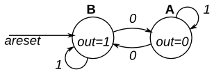
- TIPS:
状态机的代码编写方式有三种:一段式,两段式和三段式。其中一段式不推荐,常用为两段式和三段式。两段式和三段式的区别在于三段式多了一个寄存器输出,在某些情形下能够消除电路中毛刺现象。
状态机有摩尔状态机和米利型状态机。其中摩尔状态机的电路输出只与触发器的状态有关,不受电路中输入信号的影响或者没有输入信号;而米利型状态机则不仅仅与触发器的状态有关,还受电路中的输入信号的影响。由此可知,摩尔状态机只是米利型状态机的特例。module top_module( input clk, input areset, // Asynchronous reset to state B,异步置零 input in, output out);// parameter A=0, B=1; reg state, next_state; always @(*) begin // This is a combinational always block,组合逻辑 // State transition logic case(state) A:next_state = in ? A : B; B:next_state = in ? B : A; endcase end always @(posedge clk, posedge areset) begin // This is a sequential always block,时序逻辑 // State flip-flops with asynchronous reset if(areset) state <= B; else state <= next_state; end assign out = state; // Output logic //输出逻辑,根据当前状态实现输出
endmodule
### Simple FSM 1(synchronous reset)
 * **question & answer**
这是一个具有两个状态、一个输入和一个输出的摩尔状态机。实现这个状态机。请注意,重置状态为 B。同上练习一样,但使用同步复位
<div align=center><img src="https://hdlbits.01xz.net/mw/images/7/70/Fsm1.png " width="80%" height="80%"></div>

```verilog
// Note the Verilog-1995 module declaration syntax here:
module top_module(clk, reset, in, out);
    input clk;
    input reset;    // Synchronous reset to state B
    input in;
    output out;//
    reg out;

    // Fill in state name declarations
    parameter A=0,B=1;
    reg present_state, next_state;

    always@(*)begin
        case(present_state)
            A:next_state = in?A:B;
            B:next_state = in?B:A;
        endcase
    end
    always@(posedge clk)begin
        if(reset)
            present_state <= 1'b1;
        else begin
            present_state <= next_state;
        end
    end
    assign out = present_state;
endmodule
Simple FSM 2(asynchronous reset)
- question & answer
这是一个摩尔状态机,具有两个状态、两个输入和一个输出。实现这个状态机。异步复位。
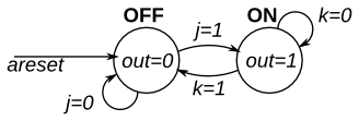
module top_module(
    input clk,
    input areset,    // Asynchronous reset to OFF
    input j,
    input k,
    output out); //

    parameter OFF=0, ON=1;
    reg state, next_state;

    always @(*) begin
        // State transition logic
        case(state)
            OFF:next_state = j?ON:OFF;
            ON:next_state = k?OFF:ON;
        endcase
    end

    always @(posedge clk, posedge areset) begin
        // State flip-flops with asynchronous reset
        if(areset)
            state <= OFF;
        else
            state <= next_state;
    end

    // Output logic
    assign out = state;

endmodule
Simple FSM 2(synchronous reset)
- question & answer
同
module top_module(
    input clk,
    input reset,    // Synchronous reset to OFF
    input j,
    input k,
    output out); //

    parameter OFF=0, ON=1;
    reg state, next_state;

    always @(*) begin
        // State transition logic
        case(state)
            OFF:next_state = j?ON:OFF;
            ON:next_state = k?OFF:ON;
        endcase
    end

    always @(posedge clk) begin
        // State flip-flops with synchronous reset
        if(reset)
            state <= OFF;
        else
            state <= next_state;
    end
    // Output logic
    assign out = state;
endmodule
Simple state transitions 3
- question & answer
下面是具有 1 个输入、1 个输出和 4 个状态的摩尔状态机的状态转换表。使用以下状态编码:A=2’b00、B=2’b01、C=2’b10、D=2’b11。仅实现该状态机的状态转换逻辑和输出逻辑(组合逻辑部分)。给定当前状态 (state),根据状态转换表计算next_state和输出 (out)。
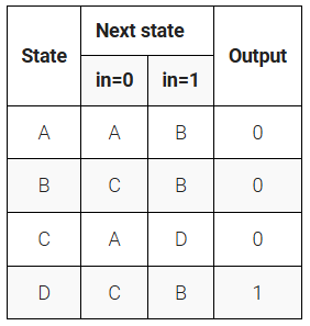
module top_module(
    input in,
    input [1:0] state,
    output [1:0] next_state,
    output out); //

    parameter A=0, B=1, C=2, D=3;

    // State transition logic: next_state = f(state, in)
    always@(*)begin
        case(state)
            A:next_state = in?B:A;
            B:next_state = in?B:C;
            C:next_state = in?D:A;
            D:next_state = in?B:C;
        endcase
    end
    // Output logic:  out = f(state) for a Moore state machine
    assign out = (state == D);
endmodule
Simple one-hot state transitions 3
- question & answer
下面是具有 1 个输入、1 个输出和 4 个状态的摩尔状态机的状态转换表。使用以下 one-hot 状态编码:A=4’b0001、B=4’b0010、C=4’b0100、D=4’b1000。
通过假设独热码的检查推导状态转换和输出逻辑方程。仅实现该状态机的状态转换逻辑和输出逻辑(组合逻辑部分)。
- TIPS:
这道题要求使用独热码,即只有一个1的编码。
这里提到了一个概念”derive equations by inspection”,指通过某一个位就可以判断当前状态,例如可以用state[0]判断当前状态是否为A,这样可以简化状态转换逻辑。
module top_module(
    input in,
    input [3:0] state,
    output [3:0] next_state,
    output out); //

    parameter A=0, B=1, C=2, D=3;

    // State transition logic: Derive an equation for each state flip-flop.
    assign next_state[A] = (state[A]&~in)||(state[C]&~in);
    assign next_state[B] = (state[A]&in)||(state[B]&in)||(state[D]&in);
    assign next_state[C] = (state[B]&~in)||(state[D]&~in);
    assign next_state[D] = state[C]∈

    // Output logic:
    assign out = (state[D] == 1);

endmodule
Simple FSM 3(asynchronous reset)
- question & answer
下面是具有 1 个输入、1 个输出和 4 个状态的摩尔状态机的状态转换表。实现这个状态机。包括将 FSM 重置为状态 A 的异步重置。
module top_module(
    input clk,
    input in,
    input areset,
    output out); //

    parameter A=2'd0,B=2'd1,C=2'd2,D=2'd3;
    reg [1:0] state,next_state;
    // State transition logic
    always@(*)begin
        case(state)
            A:next_state = in?B:A;
            B:next_state = in?B:C;
            C:next_state = in?D:A;
            D:next_state = in?B:C;
        endcase
    end
    // State flip-flops with asynchronous reset
    always@(posedge clk or posedge areset)begin
        if(areset)
            state <= A;
        else
            state <= next_state;
    end
    // Output logic
    assign out = (state==D);

endmodule
Simple FSM 3(synchronous reset)
- question & answer
同上,改为同步复位module top_module( input clk, input in, input reset, output out); // parameter A=2'd0,B=2'd1,C=2'd2,D=2'd3; reg [1:0]state,next_state; // State transition logic always@(*)begin case(state) A:next_state = in?B:A; B:next_state = in?B:C; C:next_state = in?D:A; D:next_state = in?B:C; endcase end // State flip-flops with synchronous reset always@(posedge clk)begin if(reset) state <= A; else state <= next_state; end // Output logic assign out = (state == D); endmodule